IL-7: Scanning Electron Microscopy (SEM) and application fields
A prior newsletter dealt with both function and use of the scanning electron microscopy. Now this issue provides further examples for the successful use of the scanning electron microscope (SEM) in material research and testing.
As a special possibility, the SEM of the RMS Foundation offers the three-dimensional recording and depiction of surfaces as well as the calculation of the roughness values (Ra, Rq, Rz etc.) thereof. A controlled tilting of the specimen by a few angular degrees creates this «stereoscopic view», in which one shot at different tilting angles is made each time. In addition to the three-dimensional exposition with pseudo-colours as height scale (image below) images that can be examined with 3D glasses and line profiles can be produced as well.
![]()
![]()
We defined a cross-sectional profile along the red line in the above image and depicted it below after filtering of the waviness. The thus established roughness values are Ra = 140 nm and Rz = 446 nm.
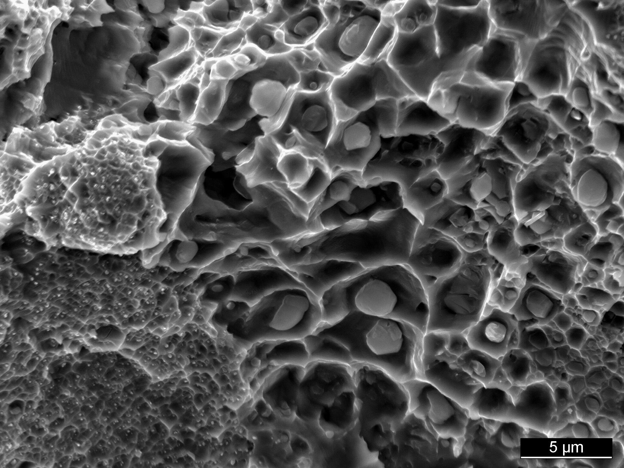
One of the most prevalent uses of the scanning electron microscopy is the failure analysis. Here, the SEM is mostly used to analyse the fracture surfaces. We can establish the reason for the failure by a systematic analysis of the material damages regarding the type of fracture (fatigue fracture, overload rupture), the initiation and the propagation of the crack as well as other possible factors (inclusions, surface defects). The following example shows a fatigue fracture surface with the typical striations.

The SEM is used as well for the characterisation of structures. We show here an etched ceramographic section as an example. The light microscope cannot expose the extremely fine-grained structure of a dispersion ceramic of aluminium oxide and zirconium oxide in the sub micrometer range.

The following image comes from an examination of a drill bit with a hard wear protection coating (thin layer). The slightly porous layer shows many fissures in the proximity of the breaking edge. Yet, the fact that there are hardly any layer chips indicates a good coating adhesion.

Equipments:
Scanning Electron Microscope (SEM)
Zeiss EVO MA25 with secondary and electron backscattered diffraction detector
• Enlargement: 5 to 150.000 times (theoretically up to 900.000 times), lateral resolution 3nm
• Materials: Polymers, metals, ceramics, minerals
• Variable pressure up to 400 Pa chamber pressure (for non-conductive specimens)
• Maximum specimen size 100 x 100 x 50mm (even larger specimens are possible in special cases)
Energy dispersive X-ray analysis (EDX)
INCA Energy 350 with Li(Si)-Link detector and super ATW window
• Qualitative analysis of all the elements from beryllium to uranium
• Quantitative analyses
• Lateral resolution: About 1µm, depending on the specimen composition
• Detection limits: Elements lighter than aluminium ≈ 0.4 – 0.5%
Elements heavier than aluminium ≈ 0.2 – 0.3%
• Mapping: Element distribution images (qualitative and quantitative)
• Linescan: Concentration profiles (qualitative and quantitative)
