In the scanning electron microscopy, we use a focussed electron beam to scan the surface of a specimen in vacuo. This emits the secondary electrons (SE) and the backscatter electrons (BSE) on the surface and records them with detectors. In the SE image the surfaces inclined towards the detector appear brighter than those turned away from the detector (surface inclination contrast). The heavier elements reveal a stronger backscattering, so that the corresponding areas appear brighter in the BSE image, whereas lighter elements are darker (material contrast image).
In the SEM we use the characteristic X-rays to distinguish the element composition of large specimen areas but of the smallest zones as well. The appropriate detectors permit to record the intensities of the characteristic X-rays and to analyse qualitatively and quantitatively the material composition of the spectra.
Examples of SEM assays


The SE image (above) shows the surface topography. The BSE image of the same location (2nd image) depicts lighter elements as darker areas. In this case the triangular foreign particle on the surface is a residue of a blasting agent. The EDX spectra of the particle (spectrum 1, aluminium oxide) and the basic material (spectrum 2, titanium) confirm the difference in the chemical composition.
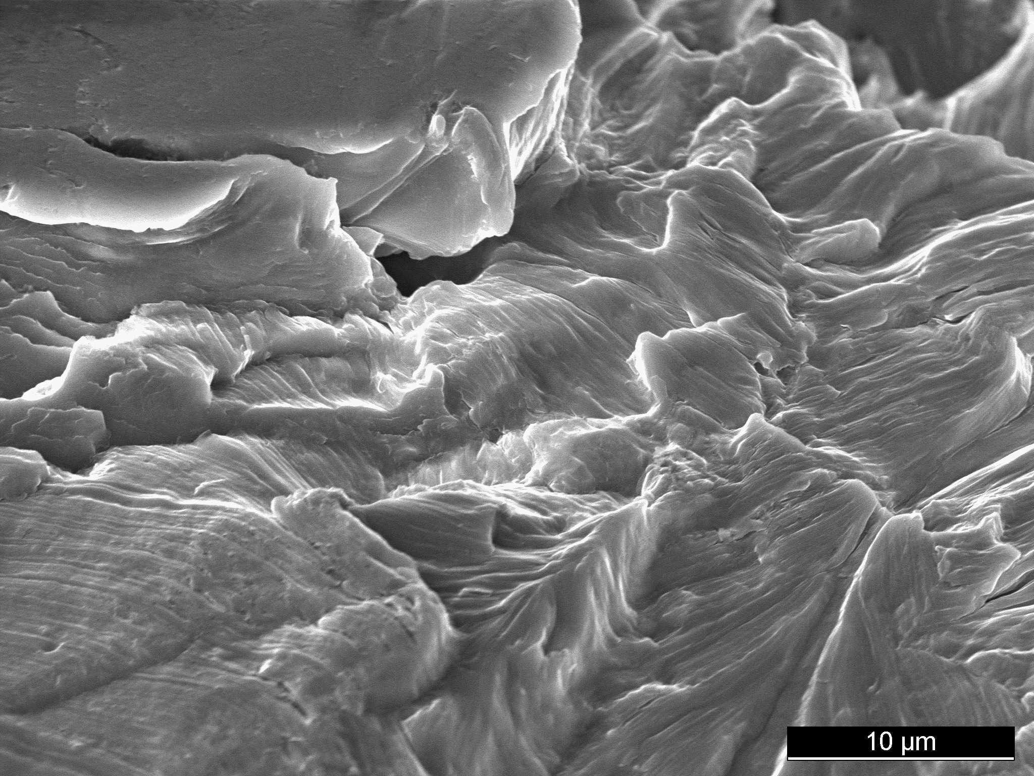
The following image very clearly shows the performance of the SEM in the exposition of topologies in the platelet structure of a form made of calcium hydrogen phosphate (Monetit).
We will go into further examples of SEM assays in a later RMS Newsletter. In particular we will elucidate more precisely the possibility of calculating the surface roughness from SEM images.
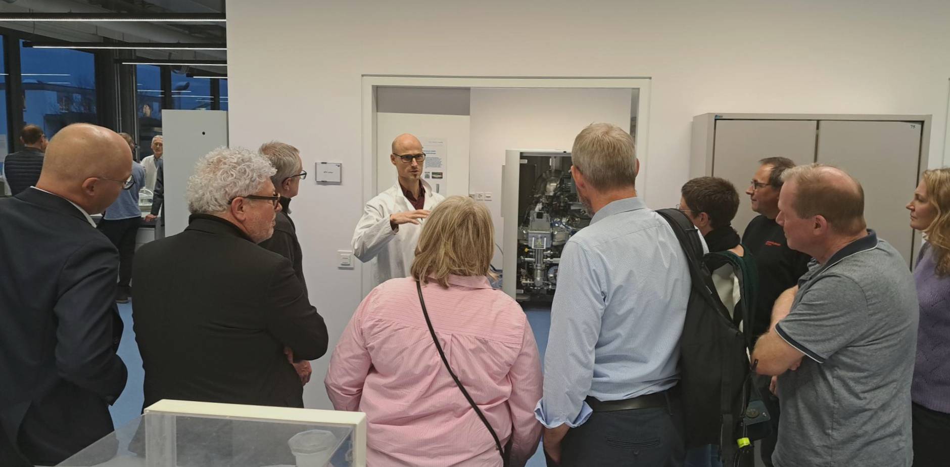
Important: Our customers have the possibility to be present during the SEM assays. This facilitates the communication and permits a situational reaction to the assay results. Very often this has a positive influence on the quality of the results.

Equipments:
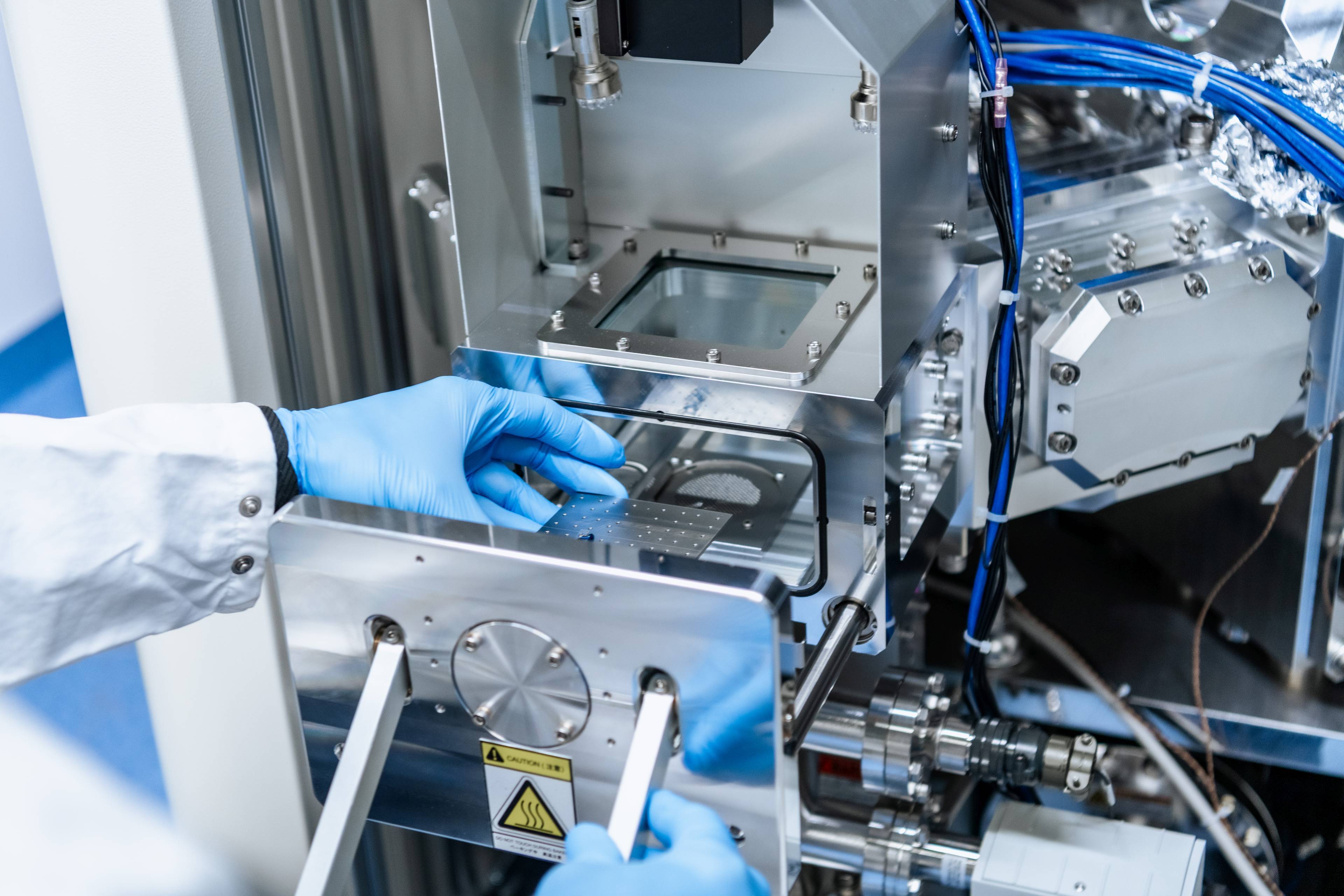
Scanning Electron Microscope (SEM)
Zeiss EVO MA25 with secondary and electron backscattered diffraction detector
• Enlargement: 5 to 150.000 times (theoretically up to 900.000 times), lateral resolution 3nm
• Materials: Polymers, metals, ceramics, minerals
• Variable pressure up to 400 Pa chamber pressure (for non-conductive specimens)
• Maximum specimen size 100 x 100 x 50mm (even larger specimens are possible in special cases)
Energy dispersive X-ray analysis (EDX)
INCA Energy 350 with Li(Si)-Link detector and super ATW window
• Qualitative analysis of all the elements from beryllium to uranium
• Quantitative analyses
• Lateral resolution: About 1µm, depending on the specimen composition
• Detection limits: Elements lighter than aluminium ≈ 0.4 – 0.5%
Elements heavier than aluminium ≈ 0.2 – 0.3%
• Mapping: Element distribution images (qualitative and quantitative)
• Linescan: Concentration profiles (qualitative and quantitative)

![Save the date - [MEET THE EXPERT] Implants](https://www.rms-foundation.ch/hubfs/01%20Bilder%20-%20Logos%20-%20Icons/Bilder%20MtE/Banner_MtE.jpg)