The MID technology combines electrical and mechanical functions in a single component. Conductor tracks are in this case placed directly on the component surface and thus replace the conventional printed circuit board. Number of parts, weight, installation space (miniaturization) and costs can be effectively reduced. In addition, many functions can be integrated into the component: shielding, cooling, heating, antenna, switches, sockets, housing, stiffeners, labels, etc.

Figure 1: Example of a 3D MID component from automotive industry: radar for adaptive speed control. The device is shown with conductor paths, but before the mounting of electronic components. Source: www.lpkf.de.
A widely used technology for the production of 3D MIDs is the Laser Direct Structuring (LDS). The LDS is based on thermoplastics that include a metal-organic complex compound as the active additive. A high-resolution circuit picture is then drawn on the injection molded part using a laser. The laser beam vaporizes the top polymer layer and activates the underlying nuclei for the metallization. In an electroless metallization step, a copper layer can then be applied specifically to the activated sites. The layer is subsequently reinforced galvanically with nickel and gold layers.


Figure 2: Materialographic sections of conductor tracks: rough thermoplastic surface (black), copper layer (reddish), nickel layer (grey), gold layer (very thin). Top image: good coating quality. Middle / bottom: irregular layer structure, polymer fragments partially embedded in the layer.
The above mentioned advantages have led to an increasing number of components that are manufactured in MID technology. They stem from the automotive, medical, automation, telecommunication, metrology, and aviation industries. The current trend is leading towards increasing miniaturization of conductor paths and spacing between them.
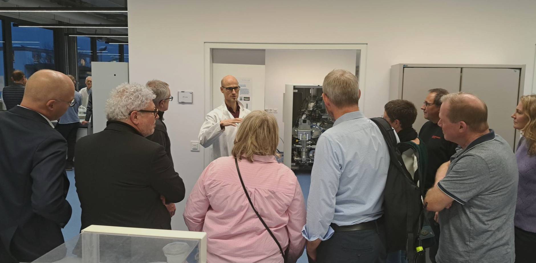
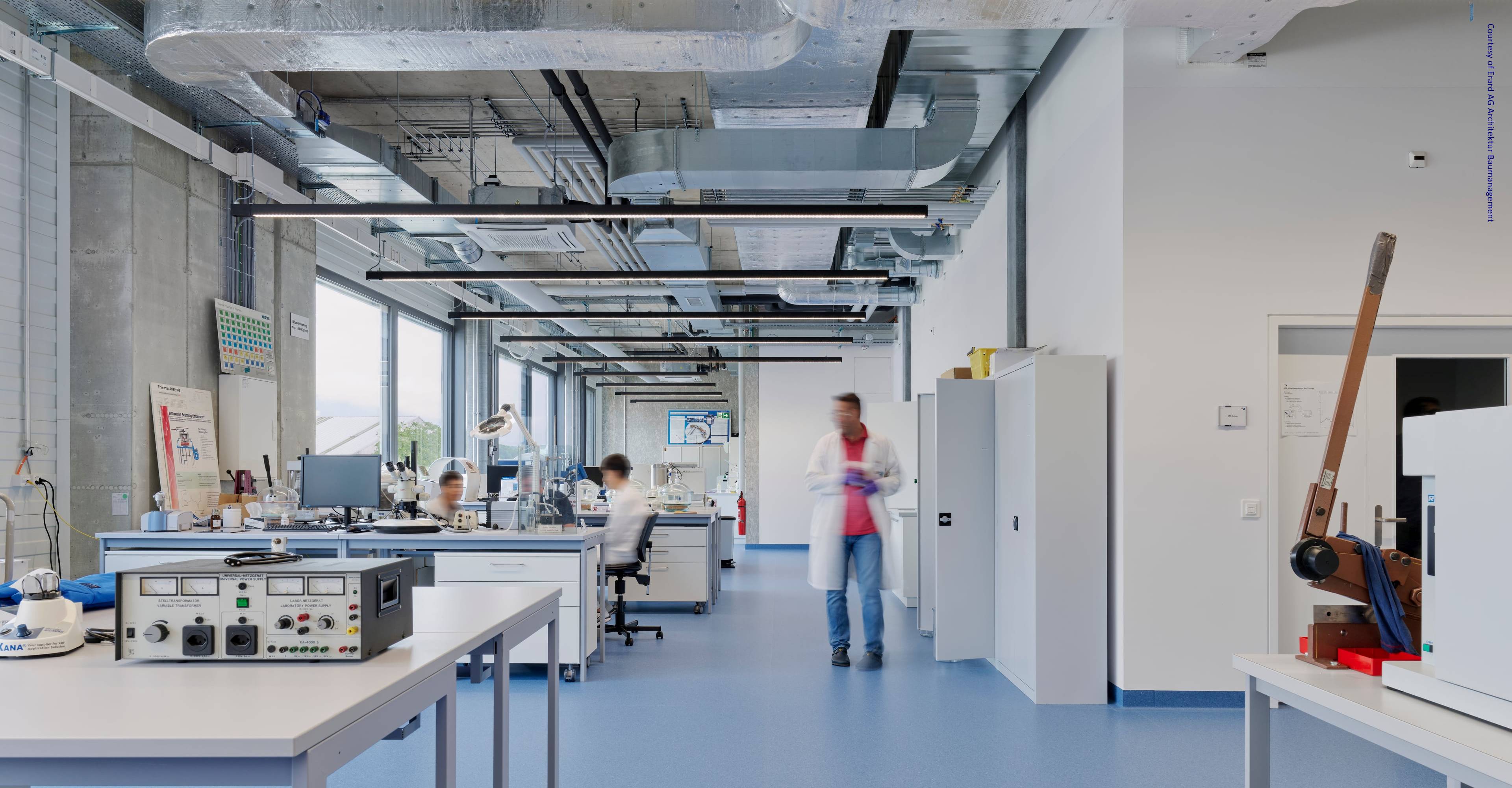
For developers and manufacturers of MID parts, the RMS Foundation offers a wide variety of services to characterize the metallization and the structure of the conductor tracks (see list at right). We can therefore make an important contribution to the further development of this technology.

Figure 3: Laser structure on the surface of the thermoplast prior to metallization.
Our services for the investigation of MIDs and other electronic components:
• Documentation of the layer structure of the interconnects with materialographic cuts.
• Studies of layer thickness, cracks in the layers, flaking and intermetallic phases.
• Analysis of the intermediate layers (contamination) with X-ray photoelectron spectroscopy (XPS) in case of adhesion problems.
• Documentation of roughness and defects with scanning electron microscopy (SEM).
• Characterization of the adhesion of layers and conductor tracks.
• Environmental testing, e.g. by cyclic temperature-humidity tests in a climatic chamber (EN 60068-2-38).

![Save the date - [MEET THE EXPERT] Implants](https://www.rms-foundation.ch/hubfs/01%20Bilder%20-%20Logos%20-%20Icons/Bilder%20MtE/Banner_MtE.jpg)